Large area CMOS image sensor design
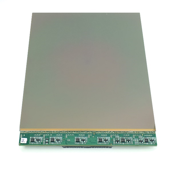
Wafer Scale Image Sensor
ISDI uses 2D stitching to create image sensors that can be almost as large as the largest rectangle that fits inside the diameter of the silicon wafer.
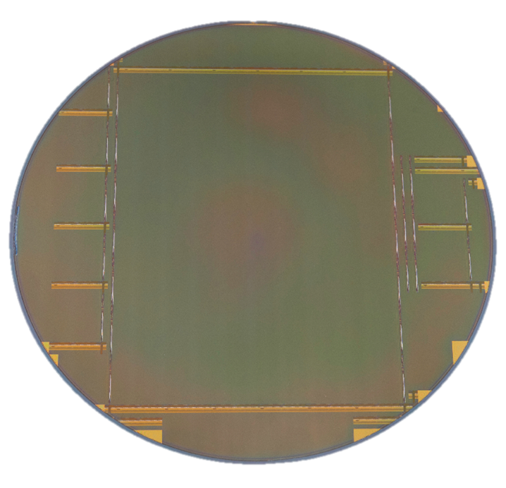
Silicon Wafer
Using stitching our image sensors can be larger than the maximum size a photo-lithography system in a fab can produce (typically around 25 mm2 for a 200 mm wafer fab). Stitching uses multiple lithographic exposures to create a single sensor. We break down the sensor design into smaller blocks, for example readout elements, edges and pixel array, and printing multiple copies of these blocks using a carefully optimised stitch plan. This stitching technology accurately aligns the blocks, allowing our large area image sensors to achieve high performance and high yields.
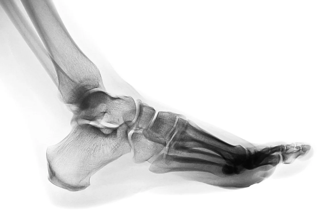
We take the process one step further by building tiled arrays of wafer-scale sensors, for example we produce the unique IS-3131 array (309 x 307 mm2) using six 153 x 103 mm2 wafer-scale sensors, which is the largest CMOS image sensor array in production.


Bonding a multiple sensor array
This array is used in the Spectrum Logic 3131HS and other X-ray detectors enabling low-dose fluoroscopy for orthopaedic and vascular surgical with unrivalled speed, field of view and image quality. This sensor has dual gain modes allowing it perform equally well in 3D computed tomography as well as real time 2D fluoroscopic radiographic imaging.