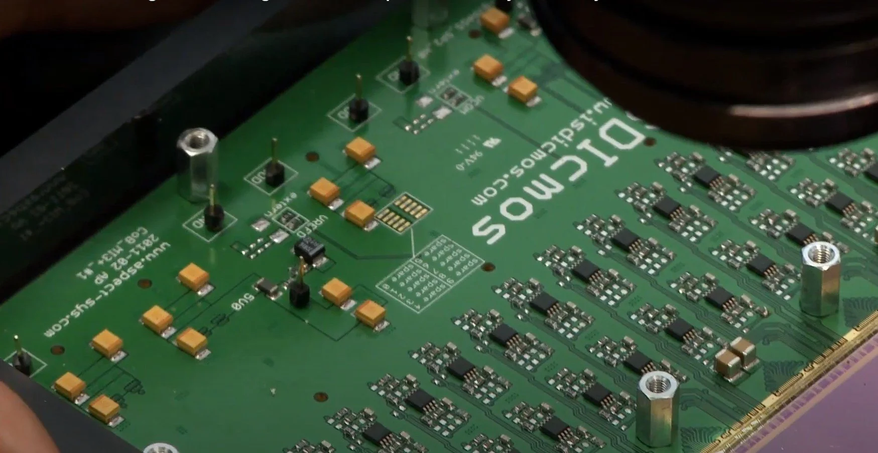
Professor Nigel Allinson MBE, one of the founders of ISDI, discusses the future trajectory of CMOS technology, in relation to Scientific and Medical imaging. Its challenges, opportunities, and its critical role in shaping next-generation of sensors and detectors. In this exclusive interview, Professor Nigel Allinson MBE shares his deep expertise and forward-looking perspectives on CMOS’s evolution in an increasingly demanding semiconductor landscape.
Read MoreFollowing his retirement in June 2025 as Distinguished Chair of Image Engineering at the University of Lincoln, we celebrated the achievements of Professor Nigel Allinson MBE, one of ISDI’s founding members. To honour his contributions, we created a series of videos (recorded last year) in which Professor Allinson discusses topics such as the origins of ISDI, scientific applications of CMOS technology, and the future of CMOS imaging.
Read MoreLarge area CMOS image sensor design: ISDI uses 2D stitching to create image sensors that can be almost as large as the largest rectangle that fits inside the diameter of the silicon wafer. Using stitching our image sensors can be larger than the maximum size a photo-lithography system in a fab can produce (typically around 25 mm2 for a 200 mm wafer fab).
Read More


